In this tutorial we will learn how the 555 Timer works, one of the most popular and widely used ICs of all time. You can watch the following video or read the written tutorial below.
Overview
The 555 Timer, designed by Hans Camenzind in 1971, can be found in many electronic devices starting from toys and kitchen appliances to even a spacecraft. It is a highly stable integrated circuit that can produce accurate time delays and oscillations. The 555 Timer has three operating modes, bistable, monostable and astable mode.
How It Works, Internal Schematic and Block Diagram
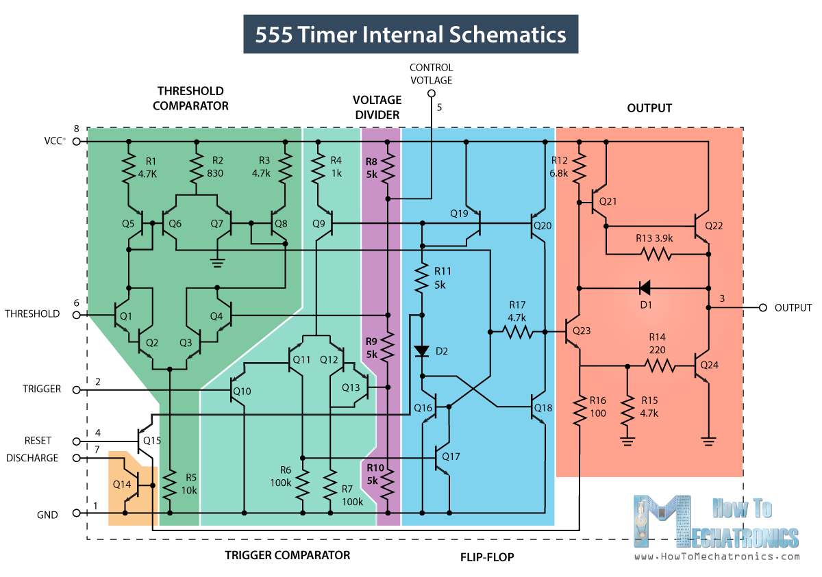
Let’s take a closer look what’s inside the 555 Timer and explain how it works in each of the three modes. Here’s the internal schematics of 555 Timer which consists of 25 transistors, 2 diodes and 15 resistors.
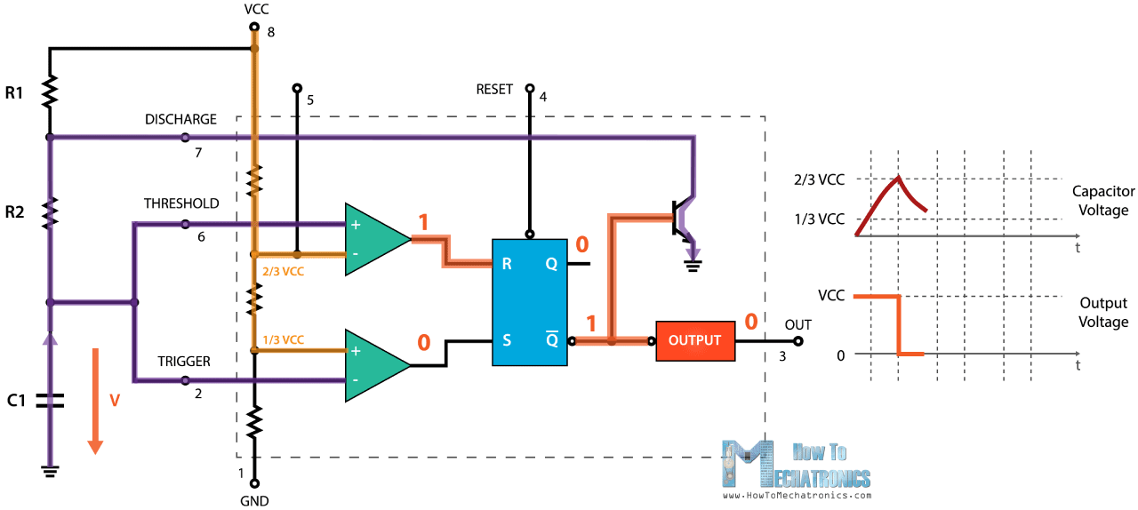
Represented with a block diagram it consists of 2 comparators, a flip-flop, a voltage divider, a discharge transistor and an output stage.
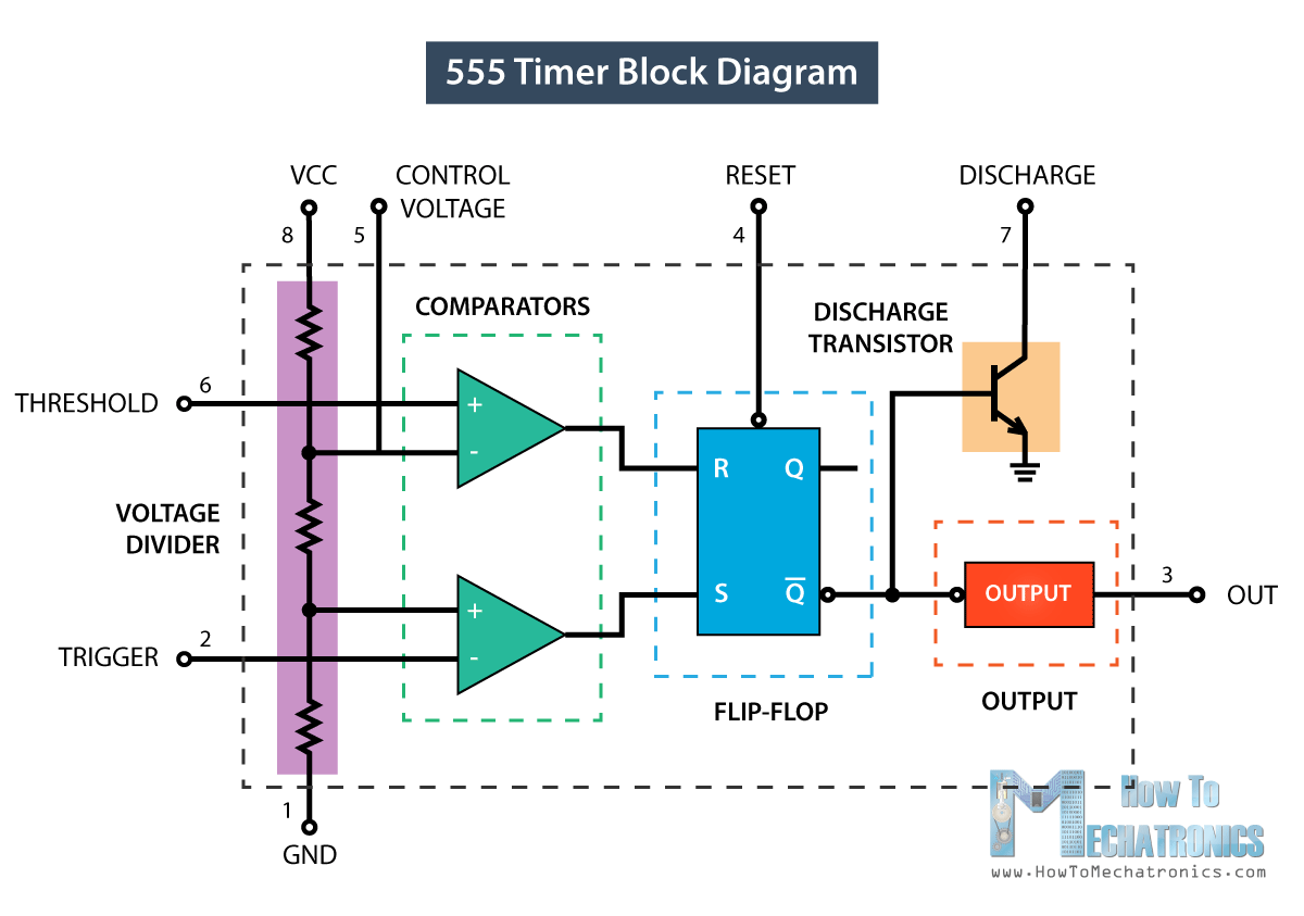
The voltage divider consists of three identical 5k resistors which create two reference voltages at 1/3 and 2/3 of the supplied voltage, which can range from 5 to 15V.
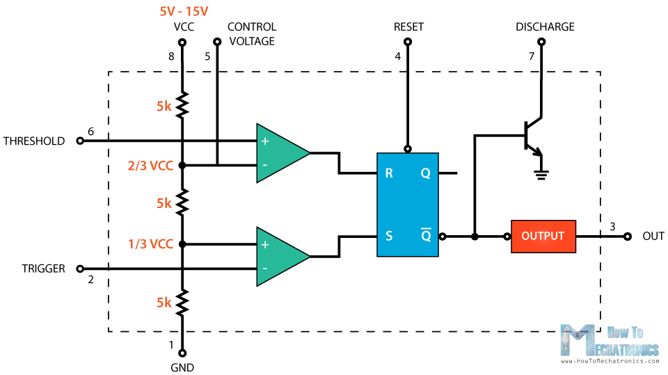
Next are the two comparators. A comparator is a circuit element that compares two analog input voltages at its positive (non-inverting) and negative (inverting) input terminal. If the input voltage at the positive terminal is higher than the input voltage at the negative terminal the comparator will output 1. Vice versa, if the voltage at the negative input terminal is higher than the voltage at the positive terminal, the comparator will output 0.
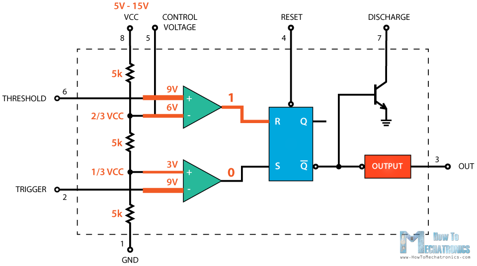
The first comparator negative input terminal is connected to the 2/3 reference voltage at the voltage divider and the external “control” pin, while the positive input terminal to the external “Threshold” pin.
On the other hand, the second comparator negative input terminal is connected to the “Trigger” pin, while the positive input terminal to the 1/3 reference voltage at the voltage divider.
So using the three pins, Trigger, Threshold and Control, we can control the output of the two comparators which are then fed to the R and S inputs of the flip-flop. The flip-flop will output 1 when R is 0 and S is 1, and vice versa, it will output 0 when R is 1 and S is 0. Additionally the flip-flop can be reset via the external pin called “Reset” which can override the two inputs, thus reset the entire timer at any time.
The Q-bar output of the flip-flip goes to the output stage or the output drivers which can either source or sink a current of 200mA to the load. The output of the flip-flip is also connected to a transistor that connects the “Discharge” pin to ground.
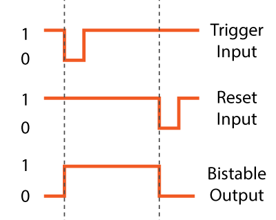
555 Timer – Bistable Mode
Now let’s make an example of the 555 Timer operating in a bistable mode. For that purpose we need two external resistors and two pushbuttons.
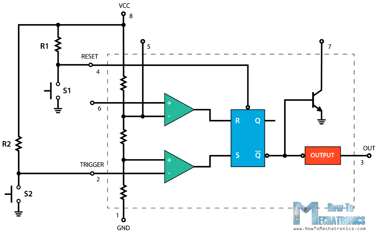
The Trigger and the Reset pins of the IC are connected to VCC through the two resistors, and it that way they are always high. The two pushbuttons are connected between these pins and the ground, so if we hold them pushed the input state will be low.
Initially, the two comparators outputs are 0, thus the flip-flop output as well as the output of the 555 Timer are 0.
If we press the Trigger pushbutton, the state at the Trigger input will become Low, so the comparator will output High and that will make flip-flip Q-bar output go Low. The output stage will invert this and the final output of the 555 Timer will be High.
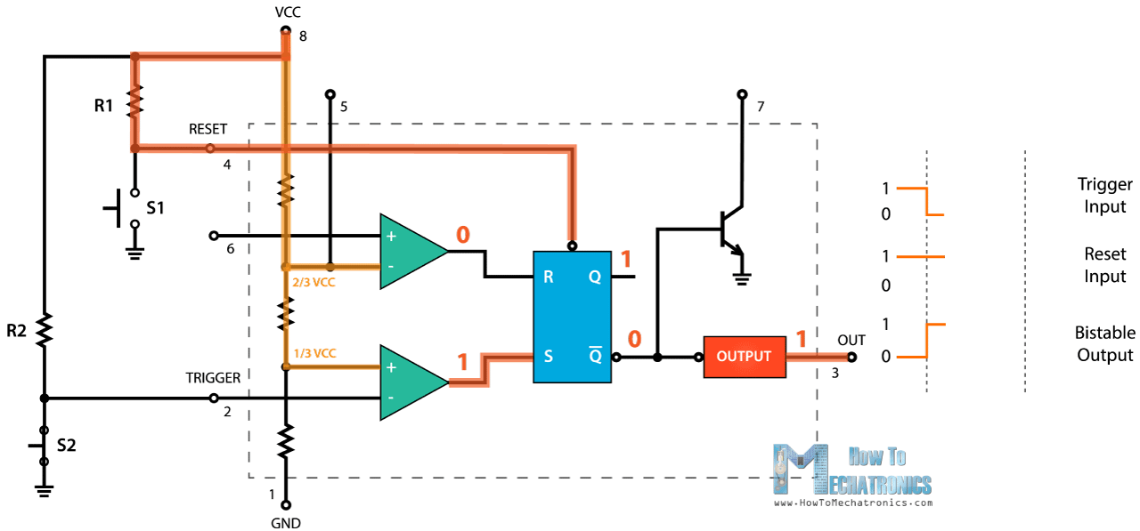
The output will remain high even when the trigger pushbutton is not pushed because in that case the flip-flop inputs R and S will be 0 which means that the flip-flop won’t change the previous state. For making the output Low we need press the Reset pushbutton, which resets the flip-flop and the entire IC.
Related tutorial: What is Schmitt Trigger | How It Works
555 Timer – Monostable Mode
Next, let’s see how the 555 Timer works in a monostable mode. Here’s an example circuit.
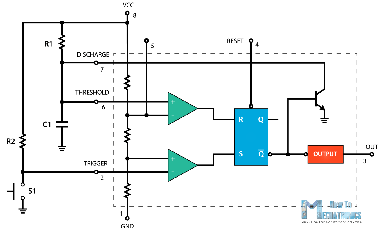
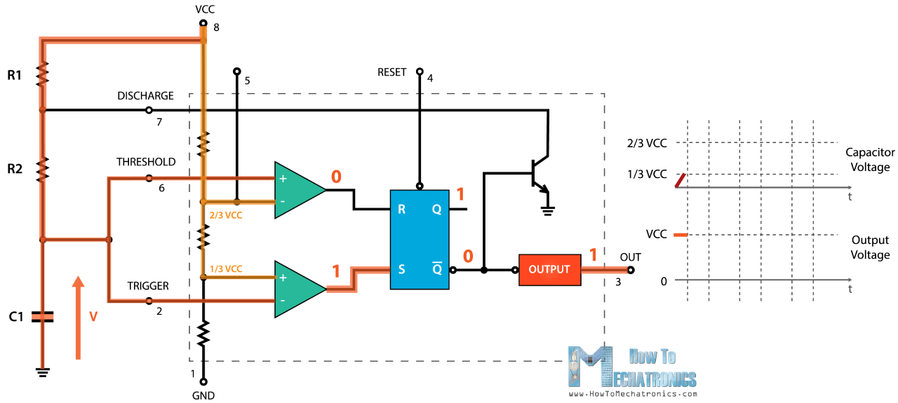
The trigger input is held High by connecting it to VCC through a resistor. That means that the trigger comparator will output 0 to the S input of the flip-flop. On the other hand, the Threshold pin is Low and that makes the Threshold comparator out 0 as well. The Threshold pin is actually Low because the Q-bar output of the flip-flop is High, which keeps the discharge transistor active, so the voltage coming from the source is going to ground through that transistor.
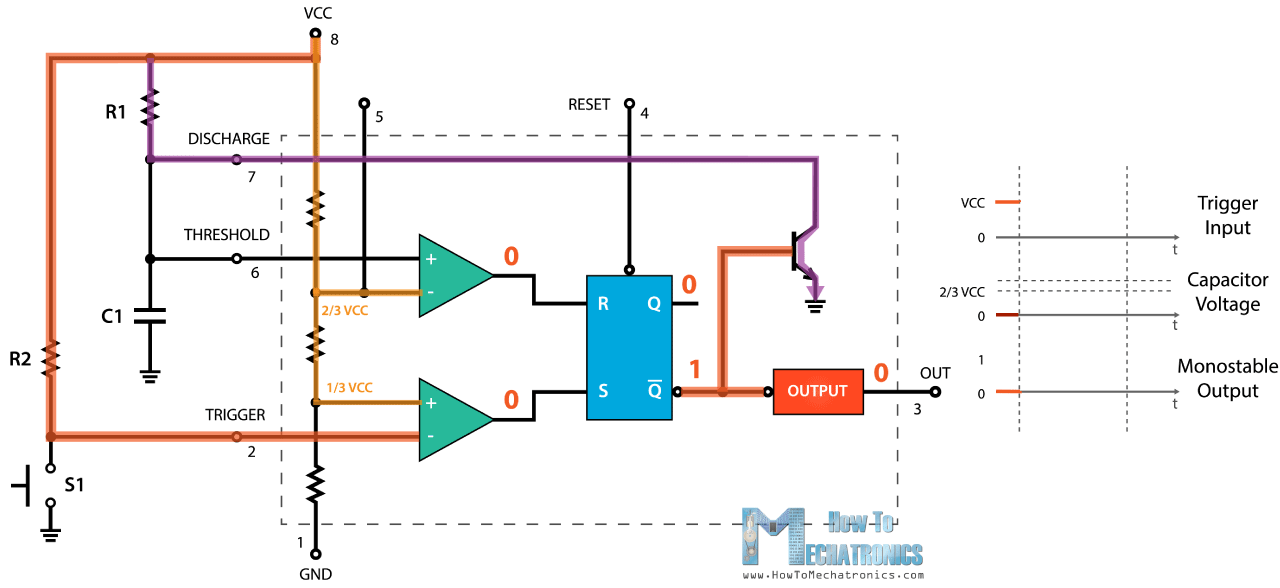
In order to change the 555 Timer output state to High we need to press the pushbutton on trigger pin. That will ground the trigger pin, or the input state will be 0, thus the comparator will output 1 to the S input of the flip-flip. This will cause the Q-bar output to go Low and the 555 Timer output High. At the same time, we can notice that the discharge transistor is turned off, so now the capacitor C1 will start charging through the resistor R1.
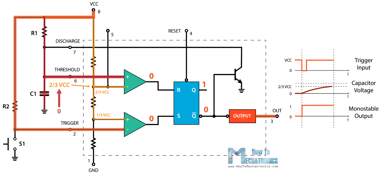
The 555 Timer will remain in this state until the voltage across the capacitor reaches 2/3 of the supplied voltage. In that case, the Threshold input voltage will be higher and the comparator will output 1 to the R input of the flip-flip. This will bring the circuit into the initial state. The Q-bar output will become High, which will activate the discharge transistor as well as make the IC output Low again.
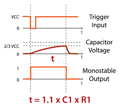
So we can notice that the amount of time the output of the 555 Timer is High, depends on how much time the capacitor needs to charge to 2/3 of the supplied voltage, and that depends on the values of both the capacitor C1 and the resistor R1. We can actually calculate this time with the following formula, T=1.1*C1*R1.
555 Timer – Astable Mode
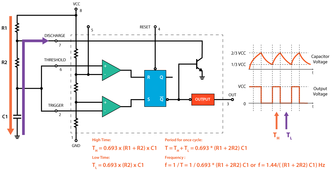
Next, let’s see how the 555 Timer works in an astable mode. In this mode the IC becomes an oscillator or also called Free Running Multivibrator. It doesn’t have a stable state and continuously switches between High and Low without application of any external trigger. Here’s an example circuit of the 555 Timer operating in astable mode.
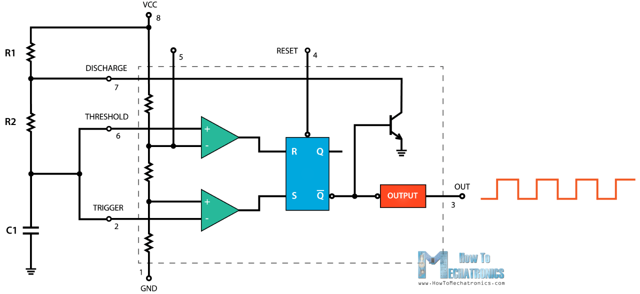
We only need two resistors and a capacitor. The Trigger and Threshold pins are connected to each other so there is no need of external trigger pulse. Initially, the voltage source will start charging the capacitor through the Resistors R1 and R2. While charging the Trigger comparator will output 1 because the input voltage at the Trigger pin is still lower than 1/3 of the supplied voltage. That means that the Q-bar output is 0 and the discharge transistor is closed. At this time the output of the 555 Timer is High.
Once the voltage across the capacitor reaches 1/3 of the supplied voltage, the Trigger comparator will output 0 but at this point that won’t do any change as both R and S inputs of the flip-flop are 0. So the voltage across the capacitor will keep rising, and once it reaches 2/3 of the supplied voltage, the Threshold comparator will output 1 to the R input of the flip-flop. This will active the discharging transistor and now the capacitor will start discharging through the resistor R2 and the discharging transistor. At this moment the output of the 555 Timer is Low.
While discharging, the voltage across the capacitor starts to decline, and the Threshold comparator right away starts to output 0, which actually doesn’t do any change as now both R and S inputs of the flip-flop are 0. But once the voltage across the capacitor drops to 1/3 of the supplied voltage, the Trigger comparator will output 1. This will turn off the discharge transistor and the capacitor will start to charge again. So this processes of charging and discharging between 2/3 and 1/3 of the supplied voltage will keep running on its own, thus producing a square wave on the 555 Timer output.
We can calculate the time the output is High and Low using the shown formulas. The High time depends the on the resistance of both R1 and R2, as well as the capacitance of the capacitor. On the other hand, the Low time depends only on the resistance of R2 and the capacitance of the capacitor. If we sum the High and Low times we will get the Period of one cycle. On the other hand, the frequency is how many times this happens in one second, so one over the Period will give use the frequency of the square wave output.
If we make some modifications to this circuit, for example, change the R2 resistor with a variable resistor or a pototentiometer, we can instantly control the frequency and the duty cycles of the square wave. However, more on this in my next video where we will make a PWM DC motor speed controller using the 555 Timer.
I hope you enjoyed this tutorial and learned something new. Feel free to ask any question in the comments section below.
Thanks very much, I am an internationally experienced industrial control geek and have had the honour of teaching basic Electronics at the local community college but, while of course I have some 555s in one of the scores – perhaps hundreds – of little plastic drawer cabinets in the basement (labeling has faded with the years but I had no trouble reading 555 and 556) I must confess that I’d forgotten what the internal block diagram looks like and my wife is building the Flola table lamp project (a young Czech designed a lamp with flower petals that are opened and closed by a stepper motor under the control of an Arduino that reads the position of a joystick in the lamp base) and the brightness is controlled by a 50K rotary potentiometer which is built into the Arduino joystick but actually has nothing to do with it: it varies the duty cycle of the 555-based astable which drives a MOSFET that sinks the LED current.
My wife has gone to bed so I did a quick search for a refresher on the 555 (I am 69 years old and I did not want to admit that I could not draw the block diagram of a 555 from memory to show her how the brightness control circuit works!)
I had already told her no need to download the circuit board mask or to order it through the project website, I could see right away that I can breadboard it relatively easily but I wanted to be able to explain what the parts that I solder to the 8-pin IC socket actually do, especially wrt the capacitor charge-discharge, so thanks for your work with this tutorial (and others that I’ll check out later) I now feel confident to draw the 8-pin “box” at the center of the schematic showing her the two comparators and the resistor ladder, the RS latch and the discharge switch (transistor) I would have been very embarrassed if I could not do that and explain for her it very simply.
Very good of you to make these tutorials available in the spirit of community that is still graces the Internet, much appreciated.
I’m so glad you found this tutorial useful. Cheers!
Nicely Explained with diagrams. It will be appreciated if you also provide step by step derivations also.